Purpose
The RT4801H is a dual output LCD bias with the input voltage range from 2.5V to 5.5V and provides 80mA output current. This document explains the function and use of the RT4801H evaluation board (EVB), and provides information to enable operation, output voltage setting of the evaluation board.
Introduction
General Product Information
The RT4801H is a highly integrated Boost and LDO and inverting charge pump to generate positive and negative output voltage. The output voltages can be adjusted from ±4V to ±6V with 100mV steps by I2C interface protocols. With its input voltage range of 2.5V to 5.5V, RT4801H is optimized for products powered by single-cell batteries and symmetrical output currents up to 80mA. The RT4801H is available in the WL-CSP-15B 1.31x2.07 (BSC) package.
Product Feature
-
2.5V to 5.5V Supply Voltage Range
-
Up to 90% Efficiency with Small Magnetics
-
Support Up to 80mA Output Current
-
Low 1µA Shutdown Current
-
Internal Soft-start Function
-
Short Circuit Protection Function
-
Over-Voltage Protection Function
-
Over-Current Protection Function
-
Over-Temperature Protection Function
-
Elastic Positive and Negative Voltage On/Off Control by ENP/ENN
-
Voltage Output from 4V to 6V per 0.1V
-
Low Input Noise and EMI
-
Output with Programmable Fast Discharge when IC Shutdown
-
Adjustable Output Voltage by I2C Compatible Interface
-
Available in the 15-Ball WL-CSP Package
Key Performance Summary Table
|
Key Features
|
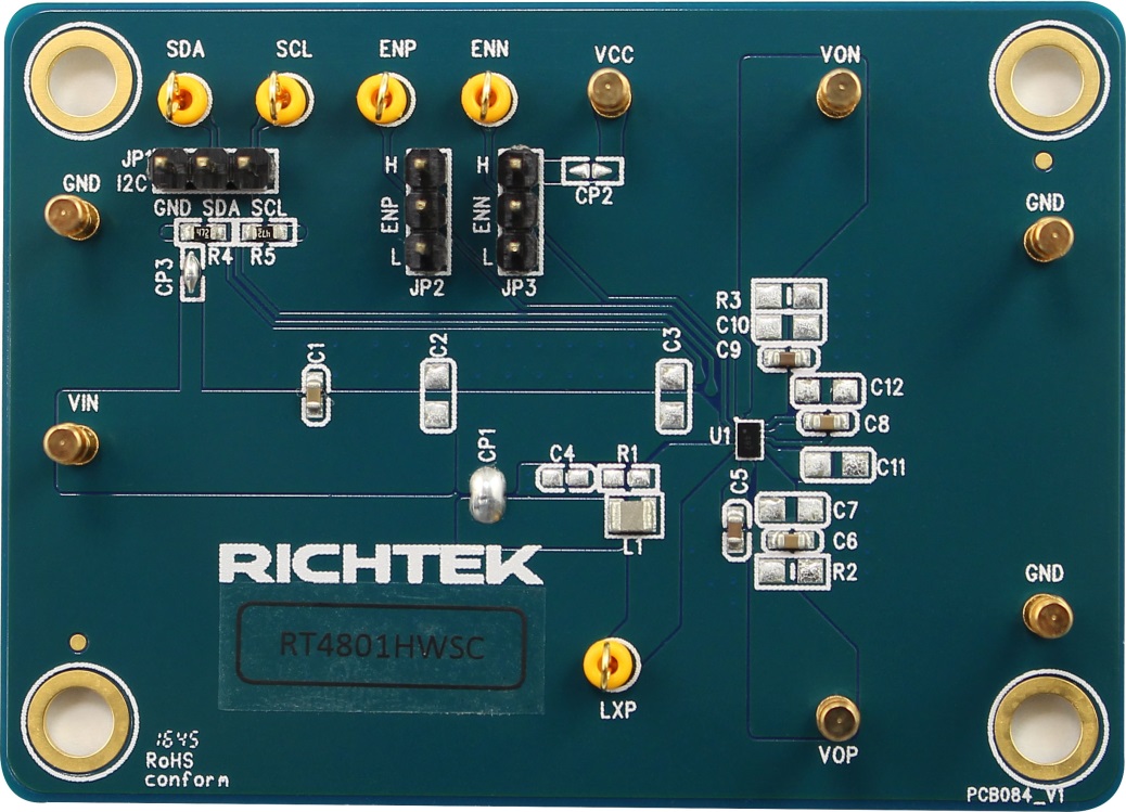
Evaluation Board Number: PCB084_V1
|
|
Default Input Voltage
|
3.7V
|
|
Max Output Current
|
80mA
|
|
Default Output Voltage
|
VOP = 5V, VON = -5V
|
|
Default Marking & Package Type
|
RT4801HWSC, WL-CSP-15B 1.31x2.07 (BSC)
|
Bench Test Setup Conditions
Carefully inspect all the components used in the EVB according to the following Bill of Materials table, and then make sure all the components are undamaged and correctly installed. If there is any missing or damaged component, which may occur during transportation, please contact our distributors or e-mail us at evb_service@richtek.com.
Test Points
The EVB is provided with the test points and pin names listed in the table below.
|
Test point/
Pin name
|
Signal
|
Comment (expected waveforms or voltage levels on test points)
|
|
VIN
|
Input voltage
|
Input voltage with range 2.5V to 5.5V.
|
|
ENP
|
VOP Enable
|
Enable control pin for VOP.
|
|
ENN
|
VON Enable
|
Enable control pin for VON.
|
|
GND
|
Ground
|
Ground.
|
|
I2C
|
I2C Control
|
Pins to set function and output voltage.
|
|
VOP
|
Positive output voltage
|
Default voltage: 5V±1%.
|
|
VON
|
Negative output voltage
|
Default voltage: -5V±1%.
|
|
LXP
|
Switching Node of Boost Converter Test Pin
|
Switching Node of Boost Converter.
|
Power-up & Measurement Procedure
Connect input voltage (2.5V < VIN < 5.5V).
1. To use a jumper at “H” option to tie ENP or ENN test pin to input voltage VIN via CP3 or external voltage via CP2 for enabling the device. Inversely, to use a jumper at “L” option to tie ENP or ENN test pin to ground GND for disabling the device.
2. To verify the output voltage VOP and VON (±5V) via I2C connector.
3. To connect an external load up to 80mA and verify the output voltage and current.
Output Voltage Setting
The output voltage can be programmed by a MCU through the dedicated I2C interface according to the VOP/VON voltage selection table. The device slave address is 0xE6.
Table1. VOP Voltage Selection
|
Name
|
Register Address
|
DATA
|
Bit7
|
Bit6
|
Bit5
|
Bit4
|
Bit3
|
Bit2
|
Bit1
|
Bit0
|
VOP (V)
|
|
VOP
|
00h
|
00h
|
Reserved
|
Reserved
|
Reserved
|
0
|
0
|
0
|
0
|
0
|
4
|
|
VOP
|
00h
|
01h
|
Reserved
|
Reserved
|
Reserved
|
0
|
0
|
0
|
0
|
1
|
4.1
|
|
VOP
|
00h
|
02h
|
Reserved
|
Reserved
|
Reserved
|
0
|
0
|
0
|
1
|
0
|
4.2
|
|
VOP
|
00h
|
03h
|
Reserved
|
Reserved
|
Reserved
|
0
|
0
|
0
|
1
|
1
|
4.3
|
|
VOP
|
00h
|
04h
|
Reserved
|
Reserved
|
Reserved
|
0
|
0
|
1
|
0
|
0
|
4.4
|
|
VOP
|
00h
|
05h
|
Reserved
|
Reserved
|
Reserved
|
0
|
0
|
1
|
0
|
1
|
4.5
|
|
VOP
|
00h
|
06h
|
Reserved
|
Reserved
|
Reserved
|
0
|
0
|
1
|
1
|
0
|
4.6
|
|
VOP
|
00h
|
07h
|
Reserved
|
Reserved
|
Reserved
|
0
|
0
|
1
|
1
|
1
|
4.7
|
|
VOP
|
00h
|
08h
|
Reserved
|
Reserved
|
Reserved
|
0
|
1
|
0
|
0
|
0
|
4.8
|
|
VOP
|
00h
|
09h
|
Reserved
|
Reserved
|
Reserved
|
0
|
1
|
0
|
0
|
1
|
4.9
|
|
VOP
|
00h
|
0Ah
|
Reserved
|
Reserved
|
Reserved
|
0
|
1
|
0
|
1
|
0
|
5
|
|
VOP
|
00h
|
0Bh
|
Reserved
|
Reserved
|
Reserved
|
0
|
1
|
0
|
1
|
1
|
5.1
|
|
VOP
|
00h
|
0Ch
|
Reserved
|
Reserved
|
Reserved
|
0
|
1
|
1
|
0
|
0
|
5.2
|
|
VOP
|
00h
|
0Dh
|
Reserved
|
Reserved
|
Reserved
|
0
|
1
|
1
|
0
|
1
|
5.3
|
|
VOP
|
00h
|
0Eh
|
Reserved
|
Reserved
|
Reserved
|
0
|
1
|
1
|
1
|
0
|
5.4
|
|
VOP
|
00h
|
0Fh
|
Reserved
|
Reserved
|
Reserved
|
0
|
1
|
1
|
1
|
1
|
5.5
|
|
VOP
|
00h
|
10h
|
Reserved
|
Reserved
|
Reserved
|
1
|
0
|
0
|
0
|
0
|
5.6
|
|
VOP
|
00h
|
11h
|
Reserved
|
Reserved
|
Reserved
|
1
|
0
|
0
|
0
|
1
|
5.7
|
|
VOP
|
00h
|
12h
|
Reserved
|
Reserved
|
Reserved
|
1
|
0
|
0
|
1
|
0
|
5.8
|
|
VOP
|
00h
|
13h
|
Reserved
|
Reserved
|
Reserved
|
1
|
0
|
0
|
1
|
1
|
5.9
|
|
VOP
|
00h
|
14h
|
Reserved
|
Reserved
|
Reserved
|
1
|
0
|
1
|
0
|
0
|
6
|
Table 2. VON Voltage Selection
|
Name
|
Register Address
|
DATA
|
Bit7
|
Bit6
|
Bit5
|
Bit4
|
Bit3
|
Bit2
|
Bit1
|
Bit0
|
VON (V)
|
|
VON
|
01h
|
00h
|
Reserved
|
Reserved
|
Reserved
|
0
|
0
|
0
|
0
|
0
|
-4
|
|
VON
|
01h
|
01h
|
Reserved
|
Reserved
|
Reserved
|
0
|
0
|
0
|
0
|
1
|
-4.1
|
|
VON
|
01h
|
02h
|
Reserved
|
Reserved
|
Reserved
|
0
|
0
|
0
|
1
|
0
|
-4.2
|
|
VON
|
01h
|
03h
|
Reserved
|
Reserved
|
Reserved
|
0
|
0
|
0
|
1
|
1
|
-4.3
|
|
VON
|
01h
|
04h
|
Reserved
|
Reserved
|
Reserved
|
0
|
0
|
1
|
0
|
0
|
-4.4
|
|
VON
|
01h
|
05h
|
Reserved
|
Reserved
|
Reserved
|
0
|
0
|
1
|
0
|
1
|
-4.5
|
|
VON
|
01h
|
06h
|
Reserved
|
Reserved
|
Reserved
|
0
|
0
|
1
|
1
|
0
|
-4.6
|
|
VON
|
01h
|
07h
|
Reserved
|
Reserved
|
Reserved
|
0
|
0
|
1
|
1
|
1
|
-4.7
|
|
VON
|
01h
|
08h
|
Reserved
|
Reserved
|
Reserved
|
0
|
1
|
0
|
0
|
0
|
-4.8
|
|
VON
|
01h
|
09h
|
Reserved
|
Reserved
|
Reserved
|
0
|
1
|
0
|
0
|
1
|
-4.9
|
|
VON
|
01h
|
0Ah
|
Reserved
|
Reserved
|
Reserved
|
0
|
1
|
0
|
1
|
0
|
-5
|
|
VON
|
01h
|
0Bh
|
Reserved
|
Reserved
|
Reserved
|
0
|
1
|
0
|
1
|
1
|
-5.1
|
|
VON
|
01h
|
0Ch
|
Reserved
|
Reserved
|
Reserved
|
0
|
1
|
1
|
0
|
0
|
-5.2
|
|
VON
|
01h
|
0Dh
|
Reserved
|
Reserved
|
Reserved
|
0
|
1
|
1
|
0
|
1
|
-5.3
|
|
VON
|
01h
|
0Eh
|
Reserved
|
Reserved
|
Reserved
|
0
|
1
|
1
|
1
|
0
|
-5.4
|
|
VON
|
01h
|
0Fh
|
Reserved
|
Reserved
|
Reserved
|
0
|
1
|
1
|
1
|
1
|
-5.5
|
|
VON
|
01h
|
10h
|
Reserved
|
Reserved
|
Reserved
|
1
|
0
|
0
|
0
|
0
|
-5.6
|
|
VON
|
01h
|
11h
|
Reserved
|
Reserved
|
Reserved
|
1
|
0
|
0
|
0
|
1
|
-5.7
|
|
VON
|
01h
|
12h
|
Reserved
|
Reserved
|
Reserved
|
1
|
0
|
0
|
1
|
0
|
-5.8
|
|
VON
|
01h
|
13h
|
Reserved
|
Reserved
|
Reserved
|
1
|
0
|
0
|
1
|
1
|
-5.9
|
|
VON
|
01h
|
14h
|
Reserved
|
Reserved
|
Reserved
|
1
|
0
|
1
|
0
|
0
|
-6
|
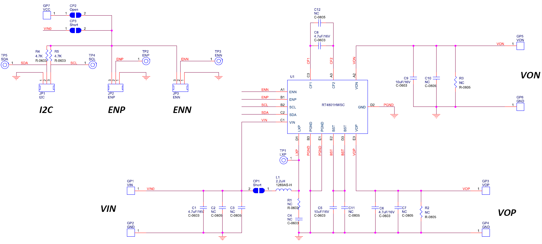
Schematic, Bill of Materials & Board Layout
EVB Schematic Diagram
Bill of Materials
|
Reference
|
Qty
|
Part number
|
Description
|
Package
|
Manufacturer
|
|
U1
|
1
|
RT4801HWSC
|
Dual Output LCD Bias IC
|
WL-CSP-15B 1.31x2.07 (BSC)
|
RICHTEK
|
|
C1, C6, C8
|
3
|
GRM188R61C475KAAJ
|
4.7µF/16V/0603
|
C-0603
|
Murata
|
|
C5, C9
|
2
|
GRM188R61C106KAAL
|
10µF/16V/0603
|
C-0603
|
Murata
|
|
L1
|
1
|
1269AS-H
|
2.2µH
|
2520
|
TOKO
|
|
R4, R5
|
2
|
RC0603JR-074K7L
|
4.7K/0603
|
R-0603
|
Yageo
|
PCB Layout
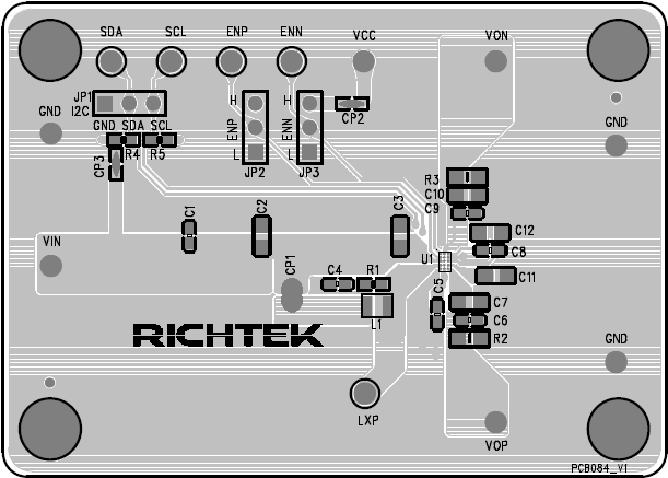
Top View (1st layer)
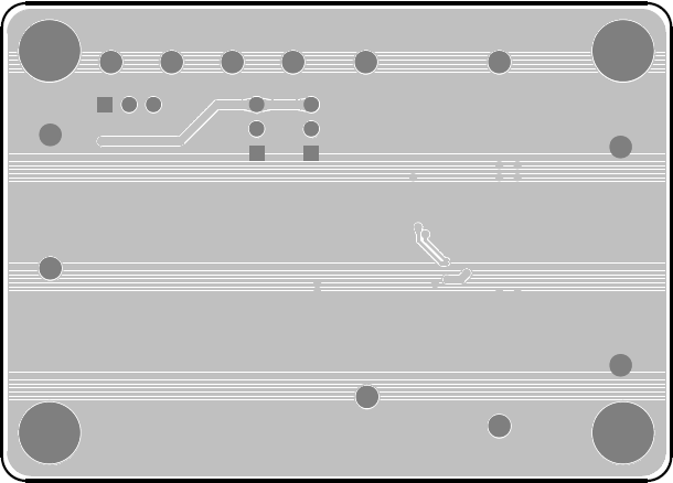
Bottom View (4th Layer)